IBM unveils world's first sub-1nm chip, halves power use
IBM created the first sub-1nm chip using NanoStack, cutting power use by half and boosting performance by 50%, proving Moore’s Law can continue. This matters because smaller, more efficient chips enab
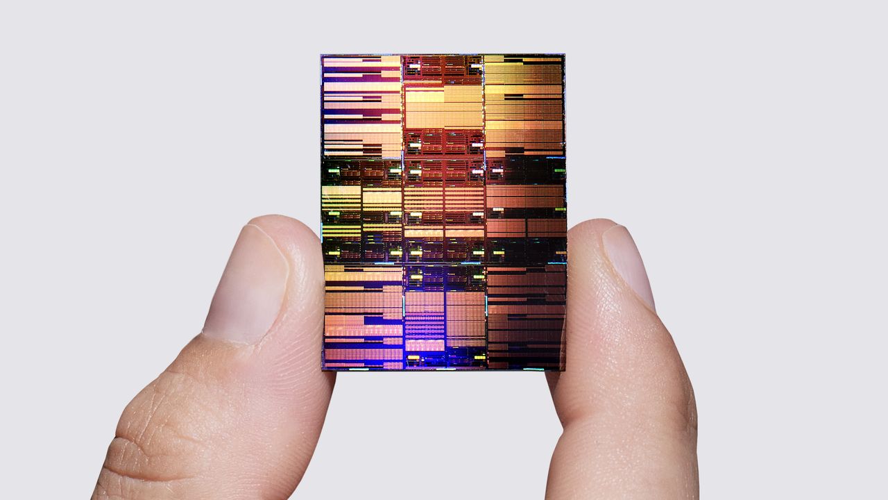
Scientists at IBM have built the world’s first computer chip with components smaller than one nanometre, halving power use and lifting performance by
Read Full Story at Live Science →Why This Matters
The breakthrough marks a pivotal moment where physical transistor scaling—long considered the backbone of computational progress—crosses into dimensions once thought impossible. Beyond raw performance gains, sub-1nm chips could redefine energy efficiency standards, making high-performance computing accessible in power-constrained environments like edge devices and renewable energy systems. If scalable, this innovation may finally silence skeptics who declared Moore’s Law obsolete, reigniting investment in semiconductor R&D at a time when global chip shortages have exposed vulnerabilities in supply chains.
Background Context
Moore’s Law has faced existential threats in recent years as classical silicon scaling hit fundamental quantum tunneling limits around 2nm. The semiconductor industry pivoted to alternative architectures—3D chips, chiplet designs, and new materials like graphene—but none matched the promise of continued miniaturization. IBM’s NanoStack approach leverages atomic-layer deposition and self-assembly techniques honed over decades, suggesting a Renaissance in lithography methods that could bypass the "red brick wall" of silicon physics.
What Happens Next
Expect a surge in R&D funding from both public and private sectors as nations and corporations scramble to replicate or adapt the NanoStack process. The next 12–24 months will reveal whether the technique can transition from lab prototypes to commercial fabrication, with yields and defect rates becoming critical battlegrounds. Meanwhile, regulatory scrutiny may intensify over environmental and ethical implications of atomically precise manufacturing, particularly if exotic materials like 2D semiconductors enter mainstream production.
Bigger Picture
This breakthrough doesn’t just revive Moore’s Law—it accelerates a broader convergence of computing and materials science, where quantum mechanics and nanotechnology blur traditional engineering boundaries. It also underscores the semiconductor industry’s shift toward "More-than-Moore" strategies, where performance gains may increasingly derive from novel device physics rather than sheer scaling. For policymakers, it’s a wake-up call: the next decade of geopolitical competition in tech may hinge on mastery of atomic-scale manufacturing, not just fabrication capacity.