PCB Trace Width, Via Current & Microstrip Impedance Calculator
IPC-2221 trace width and current, via capacity, resistance, voltage drop and microstrip impedance · free, no signup
See PCB Trace Width, Via Current & Microstrip Impedance Calculator in action
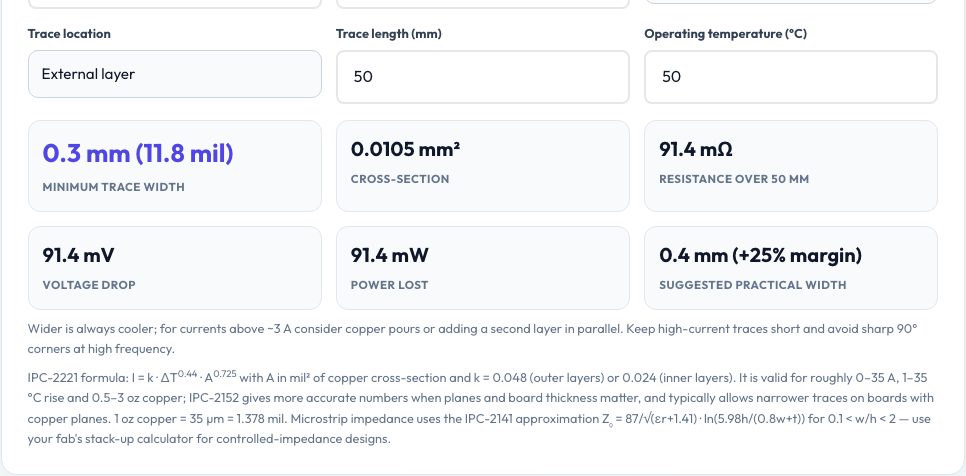
Free PCB Trace Width, Via Current & Impedance Calculator
Choosing a trace width should not be guesswork: too narrow and the trace overheats or drops too much voltage, too wide and you waste board space. This calculator uses the IPC-2221 relationship I = k·ΔT^0.44·A^0.725 to find the minimum width for a current, temperature rise, copper weight and layer position (external or internal), and the reverse — the current a given width can carry. It also shows the resistance, voltage drop and power loss over the trace length at your operating temperature, and a practical width with a 25% margin.
Further tabs estimate the current capacity and resistance of a plated via from its hole size and plating thickness, and the characteristic impedance of a microstrip from its width, height, copper thickness and dielectric constant using the IPC-2141 approximation. The IPC-2221 data is conservative for modern boards with copper planes; IPC-2152 and your manufacturer's stack-up tool give more precise figures for critical designs.
Key features
Width from current
IPC-2221 for external and internal layers, 0.5–3 oz copper.
Current from width
Maximum current for a chosen width and temperature rise.
Voltage drop and power
Resistance, drop and heat for the actual trace length.
Via and impedance tabs
Via capacity/resistance and microstrip Z₀ estimate.
How to use it
- Pick the tab and enter current, rise and copper weight.
- Read the minimum width and the practical width with margin.
- Check the voltage drop and power loss.
- Use the via and impedance tabs where relevant.
Worked example
Example
1 A on an outer layer of 1 oz copper with a 10 °C rise needs about 0.30 mm (11.8 mil); 3 A needs about 1.37 mm; a 0.25 mm trace carries about 0.9 A.
Who uses this tool
Electronics designers
Size power traces quickly.
Students
Learn the current-width relationship.
Makers
Check hobby boards before ordering.
Tips for the best results
- Use external layers for high current — they cool better.
- Add a margin: use 25–50% wider than the minimum.
- Use several vias in parallel for power paths.
- For controlled impedance use your fab's stack-up calculator.
Common mistakes to avoid
- Using internal-layer values for outer traces (too wide) or the reverse (too narrow).
- Ignoring voltage drop on long traces.
- Treating the microstrip estimate as exact.
Why use AZRS QuickFix?
It is 100% free, needs no signup and has no watermark or usage limits. The tool runs in your browser, so what you type stays on your device, and it works on phones, tablets and desktops. New tools are added every week — bookmark this page or browse the full QuickFix toolbox.
Frequently asked questions
What temperature rise should I use?
10 °C is common; 20–30 °C for tolerant designs.
What is 1 oz copper?
35 µm (1.378 mil) thick.
Is IPC-2221 still valid?
It is conservative; IPC-2152 is more accurate.
Is it free?
Yes.